Project description:
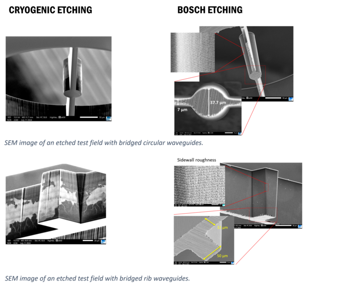
With the rapid growth of data-intensive applications such as Artificial Intelligence, the demand for efficient and high-speed chip interconnection technologies has surged. Traditional metal-based interconnects are limited by high power dissipation, latency, and crosstalk. Optical communication offers an ideal alternative with ultra-high bandwidth and reduced power dissipation. An Optical through-silicon waveguide (OTSW) is a novel, monolithically integrated solution designed to enable seamless light coupling through silicon chips, facilitating inter- and intra-chip data exchange in stacked 3D photonic architectures. This approach leverages deep reactive ion etching for scalable production, providing a simple solution for connecting nanometric silicon waveguides on multiple chip levels.
Duration: 01.06.2020 – 31.05.2025
Fördermittelgeber: Innovations- und Karrierecenter Integrated Engineering (IKC IE) (https://www.th-wildau.de/forschung-transfer/wissens-und-technologietransfer/transferaktivitaeten-projekte-und-angebote/promotion-wissenschaftlicher-nachwuchs)
Publications and patents:
- Villasmunta, F., Steglich, P., Schrader, S., Schenk, H. & Mai, A. Numerical Simulation of Optical Through-Silicon Waveguide for 3D Photonic Interconnections. In 2021 International Conference on Numerical Simulation of Optoelectronic Devices (NUSOD) (IEEE2021), pp. 115–116.
- Francesco Villasmunta, Patrick Steglich, Claus Villringer, Sigurd Schrader, Harald Schenk, Andreas Mai, and Martin Regehly "Design, fabrication, and characterization of integrated optical through-silicon waveguides for 3D photonic interconnections", Proc. SPIE 12892, Optical Interconnects XXIV, 128920I (11 March 2024); doi.org/10.1117/12.3003146
Patent application: patents.google.com/patent/US20240230990A1/en

